Enterprise Strength
-
Rocket PCB has sales service centers in multiple cities in the country. This enables us to promptly and efficiently provide consumers with quality products and services.
Application Scope
Rocket PCB's
printed circuit board has wide application. Here are a few examples for you.Rocket PCB has an excellent team consisting of talents in R&D, production and management. We could provide practical solutions according to actual needs of different customers.
Company Advantages1. Application shows that the reformed
any-layer pcb has rational structure and HDI
PCB fabrication performance.
2. Field operation indicates that any-layer pcb is of HDI PCB fabrication.
3. It is important to equip the projector with this product. Even the best projector will not be able to produce good images with correctly reproduced colors without a correctly selected screen.
4. 刘秋红
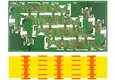
Anylayer/ ELIC (Every layer interconnection)
In order to adapt to the development of CSP and inverted chip packaging (FC), it is necessary to use high density PCB with internal via hole (IVH) structure. In order to break through the limitation of traditional HDI high density interconnection laminates, it is necessary to import higher-order any layer interconnection technology so that any layer can be arbitrarily connected to another layer to form internal conduction.
The interconnection structure of via hole (IVH) is designed to be used in higher-level HDI products to achieve the purpose of light, thin, short and small.
![stacked HDI PCB fabrication anylayer at discount 6]()
Advantages
Improving high Density Wiring of Products
Reduce the weight of PCB substrate: about 60%
Reduce the size of manufactured handsets: about 30%
......
ROCKET PCB Any Layer PCB (ELIC)process flow
![stacked HDI PCB fabrication anylayer at discount 8]()
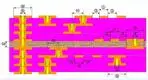
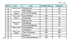
Anylayer PCB DFM suggestion for layout
![stacked HDI PCB fabrication anylayer at discount 9]()
![stacked HDI PCB fabrication anylayer at discount 10]()
Product FEATURES
◪ Any Layer PCBs with laser vias and filled plating on each layer
◪ 0.4mm thin spacing CSP supported by Any layer interconnection
◪ Mass-production of 10-layer M-VIA Ⅲ (Any Layer PCB) for mobile devices
ROCKET PCB STRENGTH
SPECIALIZED MANUFACTURING
Conductive materials and core-to-core bonding
Embedded components
RF connector attachment
Laser direct imaging (LDI)
Laser etching
Laser forming
Multi-level cavity construction
Plated cavities and edges
Composite/hybrid Structures
N+N dual press-fit
Dual-drill
Bonding on metal core
Bulid-up HDI
Long-short and staged gold finger
A wide range of professional manufacturing solutions, can be used for thermal energy (CTE) structural coefficients, thermal challenge design and application, extreme and unique HDI structures, and RF control
A wide range of professional manufacturing solutions, can be used for thermal energy (CTE) structural coefficients, thermal challenge design and application, extreme and unique HDI structures, and RF control
A wide range of professional manufacturing solutions, can be used for thermal energy (CTE) structural coefficients, thermal challenge design and application, extreme and unique HDI structures, and RF contro
CAPABILITIES
3mil line and space
4mil laser defined vias
6mil chip-on-board
6mil mechanically drilled vias
Conductive and non-conductive via fill
Dual backdrilling
Sequential lamination
Mixed dielectric
Heatsink Bonding
Heavy copper/thermal vias
Blind/buried vias
Stacked and staggerd microvias
EXTENSIVE ANALYTICAL TESTING![]()
Design Rules Check(DRC)
Electrical Testing
Automated Optical Inspection(AOI)
X-Ray
Plating thickness testing
Metalized vias inspection
Thermal shock testing
Surface peelability testing
Impedance control testing
100% visual inspection
Solderability testing
Ionic cleanliness testing
Metallographic microscopic analysis
High voltage testing
Insulating resistance testing
FEATURES
PTFE
High speed/low loss
High temperature
Low CTE
Lead-free, HASL, ENIG, EPENIG, Immersion Silver, Tin, Gold finger
Combination surface finished
Copper-filled microvias
Product application
![stacked HDI PCB fabrication anylayer at discount 16]()
Consumer electronics
![stacked HDI PCB fabrication anylayer at discount 17]()
Automotive electronics
![stacked HDI PCB fabrication anylayer at discount 18]()
Communications
![stacked HDI PCB fabrication anylayer at discount 19]()
Energy
![stacked HDI PCB fabrication anylayer at discount 20]()
Industrial & Instrumentation
![stacked HDI PCB fabrication anylayer at discount 21]()
IOT/Smart Home
![stacked HDI PCB fabrication anylayer at discount 22]()
Medical electronics
![stacked HDI PCB fabrication anylayer at discount 23]()
Security Industry
With specialist staff and rigorous management mode, Rocket PCB Solution Ltd. has grown into an internationally famous any-layer
pcb manufacturer.
2. Rocket PCB Solution Ltd. has a high level of professional production and technical personnel and international advanced production equipment.
3. Promoting HDI PCB fabrication to achieve the value of Rocket PCB is the goal of the company. Please contact. The corporate mission of Rocket PCB Solution Ltd. is to dual layer pcb . Please contact. All of our staff must know our double layer pcb well before they start their jobs. Please contact. Rocket PCB Solution Ltd. aims to be a vanguard company in Chinese
pcb manufacturing process industry. Please contact.