
Multilayer PCB generally refers to a PCB board with more than three conductive pattern layers and insulating materials laminated between them. With the development of modern electronic technology in the direction of high speed, multi-function, large capacity, and portable low power consumption, the application of multi-layer PCB has become more and more extensive, the number of layers and density are also higher and higher, and the corresponding structure is more and more complex.
Multilayer PCB is currently an essential part of the entire PCB industry. At present, the average number of layers of Rocket PCB has reached 8-20 layers, and the maximum can reach 64 layers. Both the inner layer manufacturing ability and the bonding ability are very high. S level. The emergence of multi-layer board technology is a significant development in the PCB industry, which makes the entire PCB technology advance by leaps and bounds.
What is multilayer PCB?
Multilayer board refers to a PCB that has more than three conductive pattern layers and is laminated with insulating materials between them. With the development of electronic technology to high-speed, multi-function, large capacity, and portable low-consumption direction, the application of multi-layer PCB is more and more widely, and its layer number and density are also higher and higher, and the corresponding structure is also increasingly complex. The production of multilayer PCB has become the most important part of the whole PCB industry. At present, the average number of layers of Rocket PCB has reached 8-20 layers, can up to 64 layers, which has reached a high level in terms of inner layer manufacturing ability and laminating ability. The emergence of multi-layer board technology is a major development of the PCB industry, which makes the whole PCB technology advance by leaps and bounds.
Rocket PCB is very good at multilayer PCB fabrication and prototyping. The manufacturing process of ordinary multilayer PCB is mainly based on lamination technology. Multi-layer lamination is an important process in PCB manufacturing. Rocket PCB has been producing multilayer PCBs for over 20 years. Over the years, we have seen all types of multilayer constructions from various industries, answered all types of multilayer questions, and solved all types of problems with multilayer PCBs.
Multilayer PCB Lamination
The control of lamination quality is becoming more and more important in multilayer PCB fabrication. Therefore, it is necessary to ensure multilayer laminate quality, need to have a good understanding of multilayer laminate technology. According to the processing practice for many years, Rocket PCB summarizes how to improve the laminating quality of multilayer boards as follows.
• The thickness of the core board should be selected according to the total thickness requirements of the multilayer board. The thickness of the core board should be consistent and the deviation is small.
• There should be a certain distance between the overall dimension of the core board and the effects unit, that is, the distance from the effective unit to the edge of the board should be on the premise of not wasting materials try to keep more space.
• Design of positioning hole. In order to reduce the deviation between layers, attention should be paid to the design of positioning holes in multi-layer boards: 4-layer multilayer only needs to be designed more than 3 positioning holes can be used for drilling. For multi-layer boards with more than 6 layers, in addition to designing positioning holes for drilling, it is also necessary to design more than 5 overlapping positioning rivet holes and more than 5 positioning holes for the tool plate for rivets.
• The inner core board shall be free from the open, short, open circuit, oxidation, clean board surface, and no residual film.
• Meet the requirements of PCB users, select the appropriate PP and copper foil configuration. For 4-ply laminates, 7628, 7630 or 7628 + 1080, 7628 + 2116 can be used etc. 1080 or 2116 is the main choice of PP for multilayer boards with more than 6 layers, and 7628 is mainly used to increase the thickness of the dielectric layer. At the same time, PP requires symmetrical placement to ensure mirror effect and prevent plate bending.
• Inner core board pretreatment process. The treatment process of the inner layer core board includes the black oxidation process and browning treatment process. The oxidation treatment process is to form a black oxide film on the inner copper foil, the thickness of the black oxide film is 0.25-4.50mg/cm2. The browning process (horizontal browning) is to form an organic film on the inner copper foil.
The functions of the inner laminate treatment process are as follows:
a. Increasing the surface ratio of inner copper foil and resin can enhance the adhesion between them.
b. The effective wettability of the melt resin to copper foil is increased so that the flowing resin has sufficient ability to penetrate into the oxide film and show a strong grip after curing.
c. It can prevent the decomposition of dicyandiamide in liquid resin at high temperatures and influence on the copper surface.
d. It can improve the acid resistance and prevent the PINK ring in the wet process.
e. The organic matching of lamination parameters, the control of multi-layer board lamination parameters mainly refers to the organic matching of lamination "temperature, pressure, and time". How to determine the lamination temperature, pressure, and time software parameters is the key technology for multilayer laminate processing.
Materials for making multilayer PCB
|
Various types of most commonly used FR-4 prepreg materials |
||
|
Material name |
Material type |
Original thickness (um) |
|
FR4 |
7628 |
193 |
|
2116 |
122 |
|
|
3313 |
99 |
|
|
1080 |
74 |
|
Difference between single layer and multilayer PCB
Compared with a double-layer board, the multilayer PCB has greatly improved electromagnetic compatibility.
For example, in a four-layer board, the middle layer is used as a power layer and a ground layer, and the benefits of doing so are as follows.
1. The inductance of the power wire and ground wire is greatly reduced, thus reducing the noise voltage.
2. The power supply layer and ground layer form a large distributed capacitor, which provides a good high-frequency decoupling effect for the power supply, thus reducing the noise on the power cord.
3. Independent power and ground layer can minimize the area of all signal loops.
4. PCB multilayer board is the trend of the circuit board industry, the circuit board industry is developing toward a smaller size, the smaller the hole, the thinner the thickness, the larger the number of layers, the smaller the line width and spacing, and so on.
5. Many high-precision high-tech electronic products are required multilayer PCB boards to achieve functions, the ordinary double-sided board simply cannot replace them.
Industrial printed boards (computers, instruments, etc. )
Printed circuit board for military & Aerospace
Flexible board
Rigid-Flex PCB
Blind hole board
Blind buried PCB & HDI PCB
Through-hole PCB
Printed circuit board with ceramic substrate
Metal core-based printed circuit board
In contrast, a properly constructed PCB board can effectively reduce electromagnetic radiation, crosstalk and improve signal integrity, thus providing a low inductance distribution network. According to experience, compared with a double-sided PCB board, the radiation of a four-layer board will be reduced by 15 dB. When selecting a multilayer stack, we should consider the following factors:
1) Below the surface of the component (the second layer) is the ground plane, which provides the components shielding layer and provides the reference plane for the component surface wiring;
2) All signal layers shall be adjacent to the ground plane as far as possible;
3) Try to avoid two signal layers directly adjacent;
4) The main power supply should be adjacent to its corresponding ground as far as possible;
5) In principle, a symmetrical structure design should be adopted. The meaning of symmetry includes: thickness and type of dielectric layer, the thickness of copper foil, and figure.
6) The distribution type (large copper foil layer, circuit layer) is symmetrical.
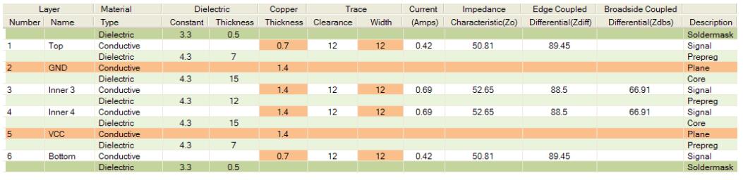
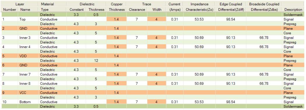
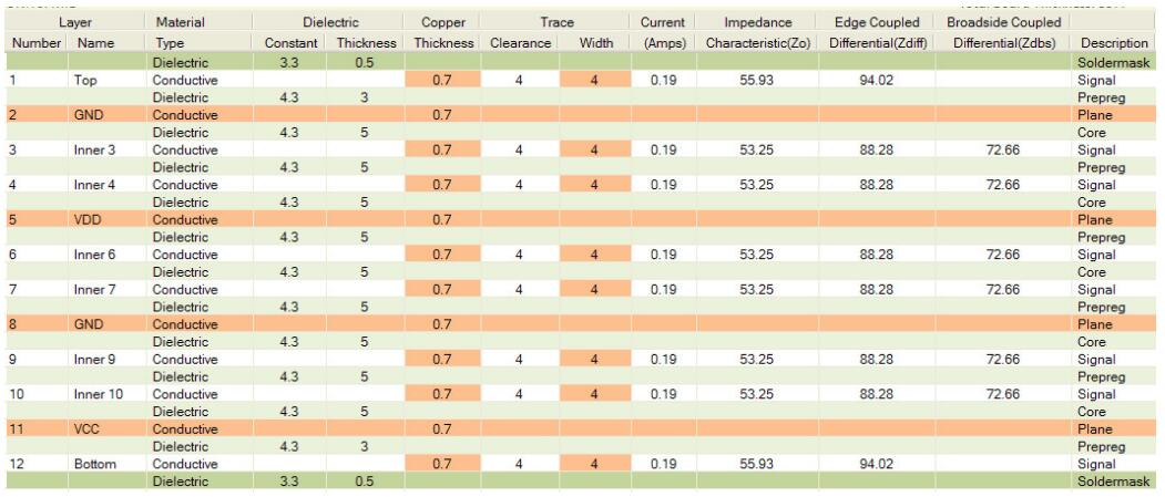
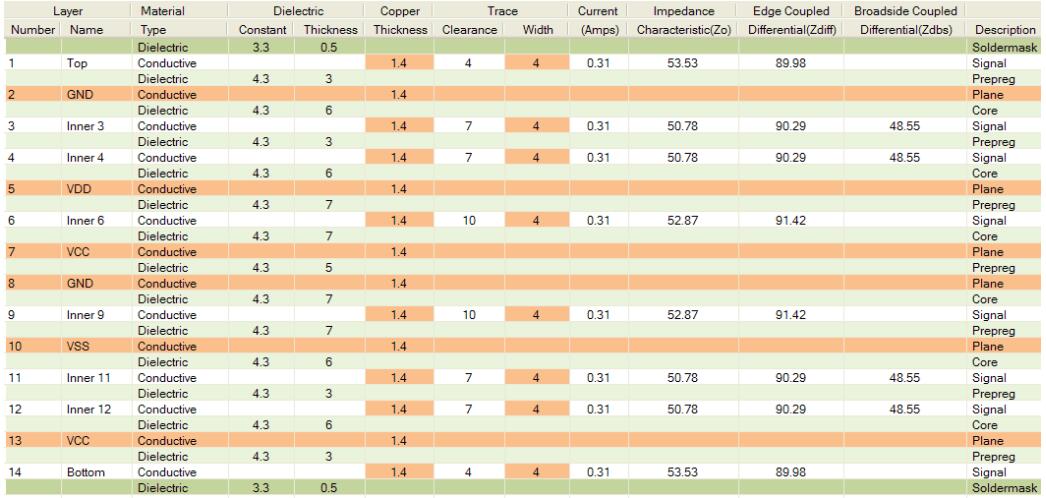
4 Layer PCB lamination A typical four layers PCB laminate is shown below.

Determine the number of layers
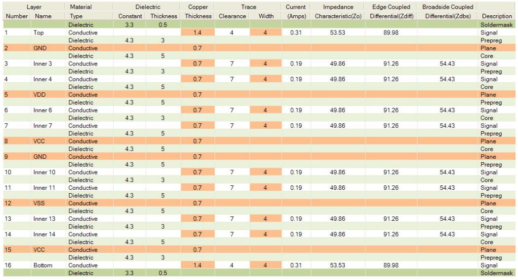
The technical rule is based on the minimum spacing of SMT components used, which is basically the maximum routing, clearance and through-hole allowed while minimizing PCB manufacturing costs. Complex high-speed designs using a ball grid array (BGA) usually require 4 / 4 mil (routing/gap) and 20 / 8 mil (PAD/hole) via technology. However, if you can, use smaller sizes, which will reduce costs and increase manufacturing output.
Once these rules are established, the required characteristic impedance (Zo) and differential impedance required stack (Zdiff) are calculated according to the component datasheet. Typically, 50 ohm Zo and 100-ohm Zdiff are used. Keep in mind that lower impedances increase the di / dt and significantly increase the absorbed current (which is detrimental to the PDN), and higher impedances generate more EMI and make the design more susceptible to external influences. Therefore, a good Zo range is 50-60 ohm.
The total number of layers required for a given design depends on the complexity of the design. Factors include the number of signaling networks that must break through from BGA; the number of power supplies required by BGA; component density and package type.
Experienced designers will know about it after a while, but checking that there are enough layers is a good way to automatically adjust the board. If not adjusted, the router needs to complete at least 85% of the routing to indicate that the selected stack is routable. You may need to reevaluate the placement several times for the best results.