


Rocket PCB customized pcb manufacturing process precision
- Rocket PCB always puts customers and services in the first place. We constantly improve service while paying attention to product quality. Our goal is to provide high-quality products as well as thoughtful and professional services.
1. Rocket PCB pcb prototyping fully complies with the relevant product safety Standard that governs it. It goes through a robust program of product testing, factory inspection, and on-going product surveillance to ensure safety.
2. The product features significant water absorption. It can absorb the amount of water under specified conditions such as temperatures and length of exposure.
3. This product is widely used by people from all walks of life.
4. The product is currently well-received in the market and is applied by more and more people.
Anylayer/ ELIC (Every layer interconnection)
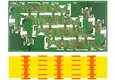
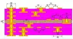
In order to adapt to the development of CSP and inverted chip packaging (FC), it is necessary to use high density PCB with internal via hole (IVH) structure. In order to break through the limitation of traditional HDI high density interconnection laminates, it is necessary to import higher-order any layer interconnection technology so that any layer can be arbitrarily connected to another layer to form internal conduction.
The interconnection structure of via hole (IVH) is designed to be used in higher-level HDI products to achieve the purpose of light, thin, short and small.
Improving high Density Wiring of Products
Reduce the weight of PCB substrate: about 60%
Reduce the size of manufactured handsets: about 30%
......
ROCKET PCB Any Layer PCB (ELIC)process flow
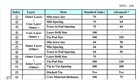
Anylayer PCB DFM suggestion for layout
Product FEATURES
◪ Any Layer PCBs with laser vias and filled plating on each layer
◪ 0.4mm thin spacing CSP supported by Any layer interconnection
◪ Mass-production of 10-layer M-VIA Ⅲ (Any Layer PCB) for mobile devices
ROCKET PCB STRENGTH
SPECIALIZED MANUFACTURING
Conductive materials and core-to-core bonding
Embedded components
RF connector attachment
Laser direct imaging (LDI)
Laser etching
Laser forming
Multi-level cavity construction
Plated cavities and edges
Composite/hybrid Structures
N+N dual press-fit
Dual-drill
Bonding on metal core
Bulid-up HDI
Long-short and staged gold finger
A wide range of professional manufacturing solutions, can be used for thermal energy (CTE) structural coefficients, thermal challenge design and application, extreme and unique HDI structures, and RF control
A wide range of professional manufacturing solutions, can be used for thermal energy (CTE) structural coefficients, thermal challenge design and application, extreme and unique HDI structures, and RF control
A wide range of professional manufacturing solutions, can be used for thermal energy (CTE) structural coefficients, thermal challenge design and application, extreme and unique HDI structures, and RF contro
CAPABILITIES
3mil line and space
4mil laser defined vias
6mil chip-on-board
6mil mechanically drilled vias
Conductive and non-conductive via fill
Dual backdrilling
Sequential lamination
Mixed dielectric
Heatsink Bonding
Heavy copper/thermal vias
Blind/buried vias
Stacked and staggerd microvias
EXTENSIVE ANALYTICAL TESTING![]()
Design Rules Check(DRC)
Electrical Testing
Automated Optical Inspection(AOI)
X-Ray
Plating thickness testing
Metalized vias inspection
Thermal shock testing
Surface peelability testing
Impedance control testing
100% visual inspection
Solderability testing
Ionic cleanliness testing
Metallographic microscopic analysis
High voltage testing
Insulating resistance testing
FEATURES
PTFE
High speed/low loss
High temperature
Low CTE
Lead-free, HASL, ENIG, EPENIG, Immersion Silver, Tin, Gold finger
Combination surface finished
Copper-filled microvias
Product application
Company Features
1. For several decades, Rocket PCB Solution Ltd. has been engaged in the pcb manufacturing processindustry, and it has grown quickly.
2. Facing the future, Rocket PCB is committed to using the leading technology to offer the best any-layer pcb .
3. Rocket PCB Solution Ltd. will focus on the needs of each customer. Please contact. The vision and mission of our company are clear and concise. We have a plan to be a leading company in this industry within several years, and we hope our employees will help us achieve the goals and objectives through their contribution. Please contact. In the long run, Rocket PCB Solution will always create value for business partners. Please contact.