


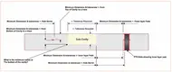


multilayer cavity pcb depth pcb
- Rocket PCB runs brand-new management and a thoughtful service system. We serve every customer attentively, so as to meet their different needs and develop a greater sense of trust.
Cavity PCB with the advantage of PCB board fabrication is widely applied. With quality and technology under control, Rocket PCB Solution Ltd. can take control of service better.
Cavity PCB plays an important role in making electronic products smaller. Compared to the standard PCB, the cavity PCB has a structural groove for additional functions. The main drivers of the cavity are thermal management and miniaturization of electronic equipment. As smaller products become more popular, more and more of our customers are seeking PCB cavity technology from us.
PCB with cavities provides space for electronic components such as capacitors, transistors, and logic modules, giving the assembled PCB an overall thinner structure. They can be applied to multilayer PCBs and they offer different layouts with several cavities of different depths if used on a single circuit board.
PCB manufacturers provide multiple ways to create a PCB cavity. Most cavity PCBs are manufactured with a controlled depth routing process equipped with a special routing machine. If required, the cavity can be electroplated. Another way to produce cavities is through sequential lamination with low-flow or no-flow prepress. The third method is through laser depth control. Rocket PCB has partnered with strong suppliers who have done great research work of PCB cavities. With the growing trend of small products, we strive to develop more new types of technology to manufacture smaller products and have attracted more customers to use our PCB cavities. Please contact us today to find out what we can help you with.
Cavity PCB types
PTH cavity with edge plating
NPTH cavity
Half-PTH cavity (pattern on bottom+SM on bottom+No plating on edge)
Cavity PCB Product Cases
Fig1 Board edge cavity with Gold Finger (Stepped edge)
Fig2 Different Cavity structure with PTH or NPTH
Typical Index | Typical value |
Layers | ≤20 |
Size | ≤247*446mm |
Total Thickness | ≤4.0 mm |
Cavity types | A. Edge plating (PTH plugging, no SM on cavity bottom) B. No plating on edge +no pattern on bottom C. No plating on edge +pattern on bottom (PTH plugging) +SM on bottom |
Cavity Size | 3mm*7mm—200mm*200mm |
Cavity depth | ≤2.0mm |
Surface treatment | HAL not applicable |
Application | Communication, PA, RF |
The main advantages of cavity PCB are as follows
Improve the overall performance of the product
Increase the density of product assembly
Meet the high-speed and high-information requirements of communication products
Reduce the size and weight of products
Strengthen the safety of surface components
Increase the heat dissipation area
Product application
Company Features
1. Rocket PCB Solution Ltd. constantly innovates and takes a leading position in the international pcb board fabrication market.
2. Rocket PCB Solution Ltd. insists on leading the great dream of power circuit board industry development. Rocket PCB Solution Ltd. will lead the future of the PCB board fabrication market. Rocket PCB commits to making achievements in the process of producing high-frequency cavity PCB. Inquire!